 大师高级课程系列之
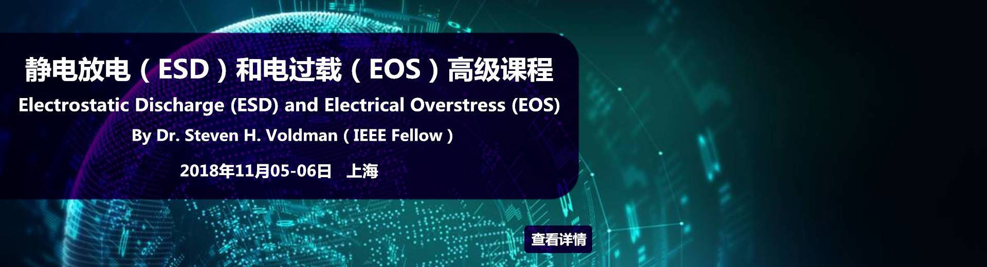
静电放电(ESD)和电过载(EOS):
器件、电路和系统 - 从先进技术到未来技术
Electrostatic Discharge (ESD) and Electrical Overstress (EOS):
Devices, Circuits and Systems – From Advanced to Future Technologies
2018年11月05日-06日 | 上海
为什么参加
随着技术从微电子技术扩展到纳米电子学,静电放电(ESD)和电过载(EOS)继续影响半导体制造、半导体元件、元器件封装和系统。本课程从组件和系统的角度讲授故障分析、测试和设计,介绍静电放电(ESD)和电过载(EOS)的基本原理。本教程提供了ESD和EOS现象、测试、电路设计和设计策略的清晰图像。本教程将介绍半导体芯片封装测试和设计方面的进展。
本次课程内容涵盖了:
• 静电放电(ESD)和电过应力(EOS)的基础知识,从物理学、时间尺度、安全工作区域(SOA)到现象的物理模型;
• 半导体器件、电路和系统中的ESD和EOS故障,讨论组件和封装的故障分析技术和工具;
• 讨论静电放电(ESD)模型和测试(例如人体模型(HBM)、带电设备模型(CDM)、电缆放电事件(CDM),带电电路板事件(CBE))到系统级IEC 61000-4 -2测试事件)以及随着系统的发展它们如何变化;
• 用于接收器、I / O、数字、模拟、混合信号和射频(RF)电路的 ESD设计;
• ESD设计版图和用于ESD电路设计的自动化设计工具;
• 展示混合信号EOS中的ESD设计和EMC故障分析扫描方法以及当前的重建技术和未来的2-D,2.5-D和3-D ESD和EOS设计问题和策略。
Electrostatic Discharge (ESD) and Electrical Overstress (EOS) continue to impact semiconductor manufacturing, semiconductor components, component packages, and systems as technologies scale from microelectronics to nanoelectronics. This course teaches the fundamentals of electrostatic discharge (ESD) and electrical overstress(EOS), from a failure analysis, testing, and design in components and systems perspective. The course provides a clear picture of ESD and EOS phenomena, testing, circuit design, and design strategies. The course will address advancements in testing and design on semiconductor chips, and packages.
The course provides extensive coverage on:
• Fundamentals of electrostatic discharge (ESD) and electrical overstress (EOS), from physics, time scales, safe operating area (SOA), to physical models for phenomena;
• ESD and EOS failures in both semiconductor devices, circuits and systems; failure analysis techniques and tools for components and packages will be discussed;
• Discussion of electrostatic discharge (ESD) events and testing (e.g. such as human body model (HBM), charged device model (CDM), cable discharge events (CDM), charged board events (CBE), to system level IEC 61000-4-2 test events) and how these are changing as systems evolve;
• ESD design of ESD circuitry for receivers, I/O, ESD power clamps for digital, analog, mixed signal, and radio frequency (RF) circuitry;
• ESD design layout and automated design tools for design of ESD circuitry;
• ESD design in mixed signal EOS and EMC scanning failure analysis scanning methods to current reconstruction techniques will be shown; and
• Future 2-D, 2.5-D and 3-D ESD and EOS design issues and strategies.
谁应该参加
本课程是为几类设计师开发的:
ESD / EMC,模拟IP模块和电路设计团队的经理及其设计人员。
ESD专家/工程师,工程师与工程/质量,系统工程师相关
具有ESD经验的设计师,更新他们的ESD知识,并根据当前的设计程序调整他们的经验。
This course has been developed for several categories of designers:
Managers of design teams of ESD/EMC, analog IP blocks and circuits, and their designers.
ESD Specialist/Engineer、 Engineers correlated with Engineering/Quality、System Engineer
Designers with ESD experience, to update their ESD knowledge and to tune their experience to the present-day design procedures.
主办单位
上海林恩信息咨询有限公司
上海集成电路技术与产业促进中心
课程安排
课程时间:2018年11月05日—06日 (2天)
报到注册时间:2018年11月05日, 上午8:30-9:00
课程地点:上海集成电路技术与产业促进中心(上海市浦东新区张东路1388号21幢)
课程费用
课程注册费用4500元/人(含授课费、场地租赁费、资料费、课程期间午餐),学员交通、食宿等费用自理(报名回执表中将提供相关协议酒店信息供选择)。
优惠折扣:在校学生注册费用3000元/人;
4人以上团体报名优惠可协商;
报名方式
请各单位收到通知后,积极选派人员参加。报名截止日期为2018年11月02日,请在此日期前将报名回执表发送Email至:
邮件:steven.yu@lynneconsulting.com
报名咨询电话:021-51096090;
或者添加微信:136 7161 3108(手机),暗号:ESD课程。
关于付款:
请于11月02日前将全款汇至以下账户。并备注(ESD课程+单位/学校+姓名)
银行信息:
户 名:上海林恩信息咨询有限公司
开户行:上海银行曹杨支行
帐 号:31658603000624127
支付宝信息:
公司名称:上海林恩信息咨询有限公司
支付宝账号:pay@lynneconsulting.com
课程具体安排
第一天: 11月05日(星期一)
Session 1: Fundamentals of ESD
• Introduction to ESD
Sources of ESD
Models
• Introduction to ESD Models
Human Body Model (HBM)
Machine Model (MM)
Charged Device Model (CDM)
Cable Discharge Events (CDE)
Transmission Line Pulse Testing (TLP)
• Introduction to Failure Models
Safe Operating Area (SOA)
Tasca Model
Wunsch-Bell Model
Dwyer Campbell Franklin Model
Session 2: Failure Mechanisms
• ESD Failures
Device Failure – MOSFET Transistor Failures
Device Failure - Bipolar Junction Transistor (BJT)
Device Failure - Heterojunction Bipolar Transistor (HBT)
• EOS Failures
Device Level
Bond Wire
Package
Printed Circuit Board
• Latchup Failures
Chip Level
Bond Wire
Package
Printed Circuit Boards
Session 3: ESD Testing
• Introduction to ESD HBM Testing
Wafer level Testing
Packaged Component Testing
Two Pin HBM Testing
• Introduction to ESD MM Testing
Wafer Level
Packaged Component Testing
• Introduction to ESD CDM Testing
CDM Test
CDM
• Introduction to ESD Transmission Line Pulse (TLP) Testing
Sources of ESD
TLP Methodology
• Introduction to ESD Very Fast Transmission Line Pulse (VF-TLP) Testing
Sources of ESD
VF-TLP Methodology
Session 4: System Level Testing
• Introduction to ESD/EMC
Scanning Methods
Scanning Method of Populated PCB
Scanning Method of Unpopulated PCB
• System Level Current Reconstruction
Methodology
Current Reconstruction Results
第二天: 11月06日(星期二)
Session 5: ESD Circuits
• I/O Receiver Networks
HBM Circuit
HBM – Diode Based Networks
HBM – MOSFET Based Networks
• I/O Receiver Networks and CDM Circuits
CDM Circuit
CDM – Diode Based Networks
CDM– MOSFET Based Networks
• ESD Power Clamps
MOSFET RC Triggered Power Clamps
Bipolar ESD Power Clamps
GGNMOS ESD Power Clamps
Floor planning
Session 6: ESD Layout and Design – Floor planning
• Analog ESD Circuits
Analog ESD Design Practices
Analog ESD Networks
• Radio Frequency ESD Circuits
RF Design Practices
RF I/O ESD Circuits
RF ESD Power Clamps
Session 7: ESD Layout and Design – Floor planning and Placement
• Digital ESD Circuits
Digital ESD Design and Layout
Digital Circuit Placement Practices
• Radio Frequency ESD Circuits
RF Design and Layout Practices
RF I/O ESD Circuits
RF ESD Power Clamps
• Analog ESD Circuits
Analog – Digital Mixed Signal
Analog ESD Design Practices
Analog ESD Networks
Session 8: ESD and Latchup
• Latchup Mechanism
Latchup Theory
Parasitic Transistors
Latchup and CMOS
• Latchup Mechanism and Placement
Latchup and Guard Rings
Latchup and I/O
ESD and I/O Placement
I/O to Core Placement
Digital-Analog-RF Placement
Session 9: ESD Design Strategies
• ESD Design
Hand Design
Automated Design Methodologies
Parametrized Cell ESD Design
• ESD Checking and Verification
Methodology
• ESD Corporate Design Practices
ESD Ground Rules
ESD Design Manual Documents
ESD Design Cookbooks
ESD Checking and Verification
Q & A: Related Problems faced by Participants
教授简介:
Steven H. Voldman博士
静电放电(ESD)领域的第一位IEEE Fellow
中文版的ESD:电路与器件;ESD:射频(RF)技术与电路;ESD设计与综合原著作者
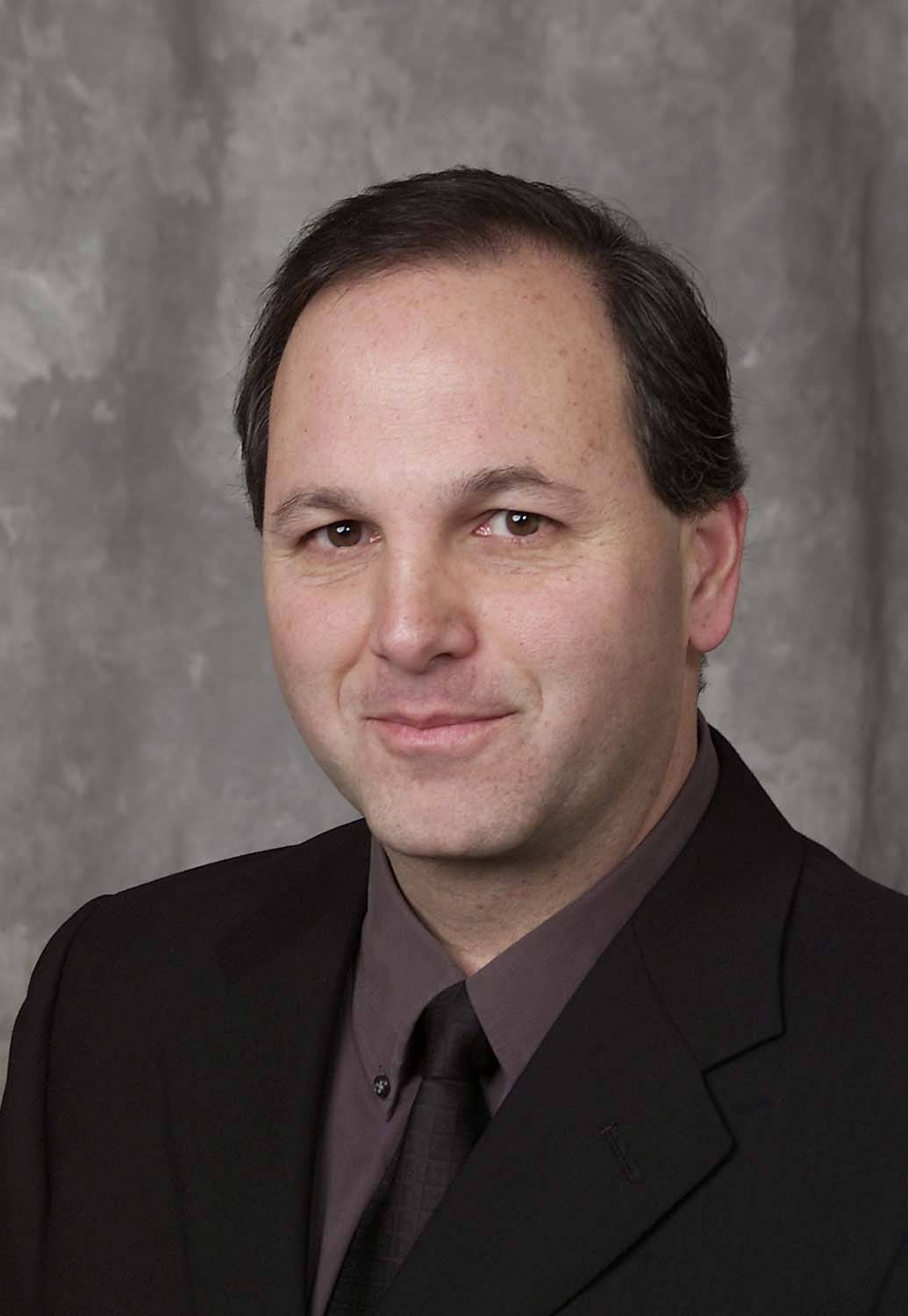 Steven H. Voldman博士静电放电(ESD)领域的第一位IEEE Fellow,基于对CMOS、绝缘体上硅和硅锗技术的ESD保护贡献。他1979年在布法罗大学工程科学专业获得学士学位;1981年获得来自麻省理工学院(MIT)EE第一个硕士学位;1986年获得第二个 Engineering Physics硕士学位,1991年获得佛蒙特大学电子工程博士学位,隶属于IBM的驻地研究员项目。Voldman是IBM、Qimonda、Intersil、TSMC、三星电子公司和Silicon Space Technology / VORAGO Corporation的半导体开发成员。他的研究和开发包括软错误率(SER)、宇宙射线、栅极感应漏极泄漏机制、DRAM泄漏、闩锁、ESD和EOS。
他发起了一个大学讲座计划,旨在为国际大学教师和学生带来讲座和互动;该计划已覆盖美国、韩国、新加坡、台湾、马来西亚、菲律宾、泰国、印度、塞内加尔、斯威士兰和中国的45所大学。 Voldman博士讲授关于ESD、闩锁、专利和发明的短期课程。 Voldman博士负责启动ESD学生章节章程,并与电子科技大学合作建立了第一个ESD协会学生章节。
Voldman博士是关于ESD、EOS和闩锁的第一本系列著作的作者(十本书):ESD:物理与器件;ESD:电路与器件;ESD:电路与器件第二版;ESD:射频(RF)技术与电路;闩锁;ESD:失效机制与模型;ESD设计与综合;ESD基础:从半导体制造到产品使用;电过载(EOS):器件、电路与系统;ESD:模拟电路与设计;ESD测试:从组件到系统;以及“硅锗:技术、建模和设计以及纳米电子:纳米线、分子电子和纳米器件”一书的撰稿人。此外,还有国际中文版的ESD:电路与器件;ESD:射频(RF)技术与电路;ESD设计与综合(2014)。
他是260项美国专利的获得者,并在ESD和CMOS闩锁方面撰写了150多篇技术论文。自2007年以来,他一直担任专利诉讼的专家证人;并且还成立了有限责任公司(LLC)咨询业务,支持专利、专利撰写和专利诉讼。在他的有限责任公司中,Voldman担任DRAM开发、半导体开发、集成电路、软件和静电放电案件的专家证人。他目前正在为律师事务所和技术公司撰写专利。 Steven Voldman在马来西亚、斯里兰卡和美国提供有关发明、创新和专利的教程和讲座。
附件下载:
1、ESD高级课程通知
2、报名注册表

 要是在成都,我就报名了。(0) 回复 (0)