

大师高级课程系列之
“Advanced Analog Circuit Design”
2016年7月04日-05日 | 北京
一、为什么参加:
由于电源电压的持续缩减,以及随着工艺尺寸的成比例缩减,器件的特性也发生了变化,模拟电路模块设计指标也在有着变化。通过学习这次课程将帮助模拟设计师提高它们设计电路的质量和鲁棒性。有机会学习怎么让你设计行之有效的模拟电路。
Design of analog circuit blocks is a moving target because of the continuing scaling of power supply voltage, and because of the changing behavior of devices with scaling of technology.
At the end of the course, it will help designers enhance the quality and robustness of the circuit they are designing. Take the opportunity and learn how to make your analog circuits perform!
二、谁应该参加:
模拟电路模块和电路设计团队的管理者和设计师。
希望巩固模拟电路知识的在校的高年级本科生、研究生,此课程需要一定的模拟电路设计基础。
Managers of design teams of analog IP blocks and circuits, and their designers.
Advanced undergraduate or graduate students who wish to develop a solid knowledge of analog circuits. A basic understanding of analog circuits is assumed.
三、主办单位:
中国国际人才交流基金会
上海林恩信息咨询有限公司
四、协办单位:
上海集成电路技术与产业促进中心
中关村芯园(北京)有限公司
五、课程安排:
课程时间:2016年07月04日—05日(2天)
报到注册时间:2016年7月04号,上午8:30-9:00
课程地点:北京外专局大厦(北京市朝阳区北四环中路华严北里8号院)
六、课程注册费用:
课程注册费用4200元/人(含授课费、场地租赁费、资料费、课程期间午餐),学员交通、食宿等费用自理(报名回执表中将提供相关协议酒店信息供选择)。
4人以上团体报名优惠可协商;
优惠折扣:在校学生注册费用3200元/人;
七、报名方式:
请各单位收到通知后,积极选派人员参加。报名截止日期为2016年06月24日,请在此日期前将报名回执表发送Email或者传真至:
邮件:steven.yu@lynneconsulting.com
传真: 021-3327-5892
报名咨询电话:021-51096090
八、课程具体安排:
第一天课程:2016年07月04日(9:00-17:00)
课题1:Low Voltage Low Power Design/低电压低功耗设计
1.Deep Submicron and Low voltage/深亚微米和低电压
深亚微米的趋势和问题简述:建模,失配,增益,干扰,速度,精度的权衡等
An overview of trends and problems towards deep submicron: modeling,mismatch, gain, interference speed accuracy trade offs
2.Low-Voltage Switched Opamps/低电压开关运算放大器
低功耗Δ-Σ转换器的设计涉及过采样率和滤波器阶数的选择,所得的动态范围也取决于具体实现,例如放大器方案,开关等。讨论一些已经优化过的低功耗,且工作电压低于1V的Δ-Σ ADC实例。
The design of low-power Delta-Sigma converters involves the choice of the oversampling ratio and the filter order. The resultant dynamic range also depends on implementation aspects such as the amplifier schemes, the switches, etc. Several examples are discussed of delta-sigma AD converters which have been optimized for low power consumption and which run at supply voltages below 1 V.
3.(A)DC-(A)DC: from Discrete Towards Fully CMOS Integrated Power management/ DC-DC:从分立器件走向全CMOS集成的电源管理技术(2节课)
学习研究全CMOS集成的DC-DC转换器的发展趋势和技术走向,分析基于电感型和电容型DC-DC变换器,讨论片上组件的不同需求,如电感。讲述不同的控制环路技术以实现高集成度,并同时实现低纹波的要求。讲述许多设计案例,并对升压型和降压型进行了分析和比较;讨论DC-DC转换器的概述及发展趋势;此外还讨论特殊的结构,如AC-DC和DC-AC转换器。
Trends and techniques towards fully integrated CMOS DC-DC converters is studied. Both inductive and capacitive DC-DC converters are analyzed. The different required on chip components such as inductors are discussed. Different control loop techniques are presented in order to achieve high integrated density and meanwhile achieving low ripple requirements. Many designed cases, both boost and buck are analyzed and compared. An overview and trend of DCDC converters will be discussed. An introduction in special structures such as AC-DC and DC-AC converters will be discussed.
第二天课程:2016年07月05日(9:00-17:00)
课题2:Essential Analog Circuit Design/模拟电路设计精粹
4.Interference Effects/干扰效应
列举并讨论RFIC中的一些EMC(电磁兼容性)干扰效应,讲解不同模块对敏感RF电路的耦合机制,研究基本模拟模块中高电源电压抑制比的设计方案。
Some EMC interference effects in integrating RF circuits are addressed and discussed. The coupling mechanism of different building blocks to the sensitive RF circuits are addressed. Design techniques for high power supply rejection ratio in basic analog building blocks are studied.
5.Interference Sources and Coupling/干扰源和耦合
分析了干扰源及其对耦合效应的影响,介绍了数字和模拟电路噪声构成的实例。对pinning策略和衬底效应进行简单地讨论,对设计规则和绑定线影响进行了研究。
Different sources and their impact on coupling effects are analyzed. Both examples of digital and analog circuit noise generating structures are presented. A brief discussion of pinning strategy and substrate effects are discussed. Design rules and bond wire effects are investigated.
6.Offset and CMRR: Random and Systematic/失调和CMRR(共模抑制比):随机性和系统性
差分结构中对称设计晶体管的随机性失配引起失调,导致CMRR/PSRR的下降。这里详细介绍了随机失配的现象,分析了其在差分对、电流镜等设计中的相关性。课程最后,给出改善匹配的一系列设计规则。
Random mismatch between the equal-designed transistors in a differential pair causes offset and reduction of both the CMRR and the PSRR. This phenomenon of random mismatch is discussed in detail. Its relevance is analyzed for differential pairs, current mirrors, etc. At the end of the session, a number of design guidelines are put together for better matching.
7.Design for EMC/ EMC设计
EMC问题的介绍:EMI,EME,EMS,电荷泵。基本模块的EMC设计技术:原理,电流镜,输入和输出结构。
Introduction to EMC problems: EMI, EME, EMS, charge pumping. EMS design techniques on basic building blocks: principles, current mirror, input and output structures.
九、教授简介:
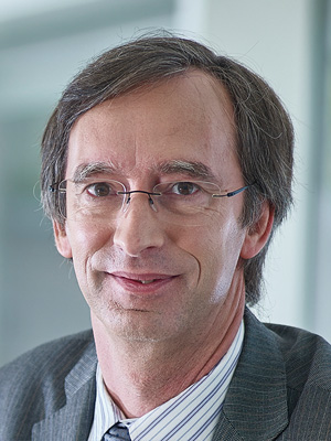
 米歇尔. 斯泰耶尔教授(Michiel S.J. Steyaert)分别于1983年和1987年获得比利时鲁汶大学电子机械工程硕士学位和电子工程博士学位。
1983年到1986年期间,他担任鲁汶大学ESAT实验室助理研究员,并获得IWNOL奖学金(比利时国家基础工业研究)。1987年,他作为IWONL项目研究员在鲁汶大学ESAT实验室负责模拟微功耗电路领域中一些工业项目。
1988年,他担任加州大学洛杉矶分校的客座助理教授,1989年他被指派为科学研究国家基金(比利时)的研究助理,1992年升为高级研究员,并在1996年担任鲁汶大学ESAT实验室研究总监。1989年到1996年期间,他也是鲁汶大学兼职副教授,现在是鲁汶大学的全职教授。2005到2012年,他曾是鲁汶大学电子机械系主任,现在他已是工程院院长。他目前的研究领域是通信系统和模拟信号处理方面高性能和高频率的模拟集成电路设计。
米歇尔. 斯泰耶尔教授与他人在国际期刊/会议上撰写/共同撰写超过500篇文章,并共同编撰了16本书。他获得了1990年和2001年的欧洲固态电路会议最佳论文奖,由于其在无线通讯集成电路设计中创新性的工作,他获得1991年和2000年 NFWO阿尔卡尔贝尔电话奖。米歇尔. 斯泰耶尔教授获得1995年和1997年的IEEE-ISSCC晚间会议奖,1999年的IEEE电路和系统学会Guillemin-Cauer奖,并且自2003年来一直是IEEE院士。因在集成电路领域突出而持久的贡献,他是仅有的一位两次获得顶级ISSCC贡献者奖的欧洲研究人员,一次是2003年第50周年,一次是2013年第60周年。
手机扫描下图课程内容信息二维码,手机查看详细课程信息及参与课程分享!
附件文件下载:
附件1:课程详细通知
附件2:课程注册表
- 还没有人评论,欢迎说说您的想法!