大师高级课程系列之
用于数字、模拟和射频(RF)应用的静电放电和闩锁设计
Electrostatic Discharge and Latchup Design for Digital, Analog and Radio Frequency (RF) Applications
2019年11月18日-19日 | 上海
为什么参加
在这个短期课程中,将讨论用于数字,模拟,混合信号和射频(RF)应用的静电放电(ESD)原理和设计。本课程将侧重于如何进行电路设计以及整个芯片的布局布线,以为产品提供最大的ESD鲁棒性,从而避免ESD失效,帮助产品在合格鉴定和发布方面获得最大的成功。该课程还将细致地区分不同芯片应用中的ESD设计实践,模拟和RF设计原则将应用于ESD设计,以为产品类型提供最佳解决方案,同时将讨论产品设计层次和架构规划。此外,本课程还将讨论数字、模拟和混合信号架构的闩锁设计和布局。课程示例、材料和发明概念将摘自作者关于ESD、EOS和闩锁的书籍。本课程与去年的ESD课程有所不同,侧重点是电路设计和布局。
In this short course, electrostatic discharge (ESD) principles, and design will be discussed for digital, analog, mixed signal, and radio frequency (RF) designs. This course will focus on how to layout and design circuits and full-chip to provide maximum ESD robustness for products to avoid ESD failures and provide maximum success in qualification and product release. The course will also provide a clear distinction of ESD design practices in different chip applications. Analog and RF design principles will be applied to ESD design to provide optimum solutions for the product types. Circuit solutions and ESD designs will be discussed and product floor planning and architecture. Additionally, the course will discuss latchup layout and design for digital, analog and mixed signal architectures. Examples and material as well as invention concepts will be drawn from the author’s books on ESD, EOS, and latchup. This course will differ from last ESD courses with an emphasis on circuit design and layout.
Upon completing this course, the participant will be able to:
- Develop a comprehensive understanding of electrostatic discharge (ESD) and latchup
- Learn about commercial designs used for digital, analog and radio frequency (RF) applications
- Learn semiconductor chip layout and architecture for full-chip protection
- Learn analog design techniques for ESD protection and optimization
- Understand the impact of ESD in semiconductor chip design in radio frequency (RF) design
- Learn about optimized circuits for performance and ESD
谁应该参加
本课程是为几类设计师开发的:
有兴趣了解静电放电(ESD)和闩锁原理和设计的数字、模拟、混合信号和射频(RF)设计人员,电路设计工程师,布局设计工程师,技术经理和对ESD保护实用设计感兴趣的研究生。
This course has been developed for several categories of designers:
Digital, analog, mixed signal, and radio frequency (RF) designers interested in understanding the principles and design of electrostatic discharge (ESD) and latchup. Circuit solutions and ESD designs will be discussed and product floor planning and architecture. Circuit design engineers, layout and design engineers, technical managers, researchers and graduate students interested in practical design for ESD protection.
主办单位
上海林恩信息咨询有限公司
上海集成电路技术与产业促进中心
课程安排
课程时间:2019年11月18日—19日 (2天)
报到注册时间:2019年11月18日, 上午8:30-9:00
课程地点:上海集成电路技术与产业促进中心(上海市浦东新区张东路1388号21幢)
课程费用
课程注册费用4500元/人(含授课费、场地租赁费、资料费、课程期间午餐),学员交通、食宿等费用自理(报名回执表中将提供相关协议酒店信息供选择)。
优惠折扣:在校学生注册费用3000元/人;
4人以上团体报名优惠可协商;
报名方式
请各单位收到通知后,积极选派人员参加。报名截止日期为2019年11月15日,请在此日期前将报名回执表发送Email至:
邮件:steven.yu@lynneconsulting.com
报名咨询电话:021-51096090;
或者添加微信:136 7161 3108(手机),暗号:ESD课程。
关于付款:
请于11月15日前将全款汇至以下账户。并备注(ESD课程+单位/学校+姓名)
银行信息:
户 名:上海林恩信息咨询有限公司
开户行:上海银行曹杨支行
帐 号:31658603000624127
支付宝信息:
公司名称:上海林恩信息咨询有限公司
支付宝账号:pay@lynneconsulting.com
课程具体安排
Day 1 Part I - ESD Design in Digital
ESD Architecture - I/O Design
ESD Receiver Design
ESD Receiver Design Practices
Single Ended Receiver Design
Differential Receivers
HBM and CDM ESD Solutions
Dual Diode
Dual Diode – Resistor – Dual Diode
ESD Off-Chip Driver Design
ESD OCD Design Practices
Standard Driver Design
Mixed Voltage Driver
Self Protecting OCD
Floating Well OCD
ESD Power Clamps
ESD Power Clamp Design Practices
CMOS RC Triggered MOSFET Power Clamps
Mixed Signal MOSFET Power Clamps
Bipolar Silicon Germanium Power Clamps
Bipolar GaAs Power Clamps
Day 1 Part II - ESD Design in Analog
How is Analog ESD Design Different From Digital ESD Design ?
Analog Design Practices
Analog Design and Local Matching
Analog Design and Global Matching
Symmetry - Layout Symmetry
Symmetry - Thermal Symmetry
Passive Design
Capacitors
Inductors
Resistors
Common Centroid Design
Analog Circuits - Voltage Regulators, Current Mirrors,Schmitt Trigger Circuits
Digital-to-Analog ESD Design Synthesis
Domain to Domain Issues
Analog ESD Design Co-Synthesis
Differential Pair and Common Centroid Design
Day 2 Part III - ESD Design in Radio Frequency Applications
How is RF ESD Design Different from Digital Design ?
RF ESD Design Practices
RF ESD Design
RF Design Methodology
Hierarchical ESD Design
Parametrized Cells
RF CMOS
Silicon Germanium
Silicon Germanium Carbon
Gallium Arsenide
Day 2 Part IV - Latchup
Latchup Design Practices
Latchup Ground Rules
Latchup Guard Rings and Guard Ring Rules
Evaluating Guard Ring Efficiency
Type of Guard Rings
N+
N-Well
Triple Well
Trench Guard Rings
Moats
High Voltage Guard Rings
TSV Guard Rings
Passive Guard Rings
Active Guard Rings
Latchup In a Common Circuit
PFET to NFET
I/O to ESD Network
I/O to ESD Power Clamp
Latchup Within an ESD Network
Latchup in RC Triggered ESD Power Clampl
Latchup I/O to I/O
Peripheral I/O Adjacent I/O
Peripheral I/O to Decoupling Capacitor
Latchup I/O to Core
Latchup Core to Core
Latchup in Array I/O Architecture
Latchup Propagation in Core
Latchup Domino Effect
教授简介:
Steven H. Voldman博士
静电放电(ESD)领域的第一位IEEE Fellow
中文版的ESD:电路与器件;ESD:射频(RF)技术与电路;ESD设计与综合原著作者
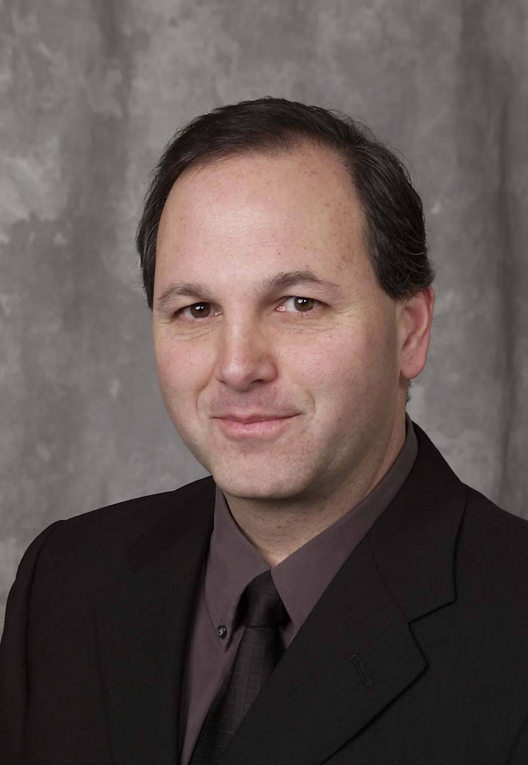 Steven H. Voldman博士静电放电(ESD)领域的第一位IEEE Fellow,基于对CMOS、绝缘体上硅和硅锗技术的ESD保护贡献。他1979年在布法罗大学工程科学专业获得学士学位;1981年获得来自麻省理工学院(MIT)EE第一个硕士学位;1986年获得第二个 Engineering Physics硕士学位,1991年获得佛蒙特大学电子工程博士学位,隶属于IBM的驻地研究员项目。Voldman是IBM、Qimonda、Intersil、TSMC、三星电子公司和Silicon Space Technology / VORAGO Corporation的半导体开发成员。他的研究和开发包括软错误率(SER)、宇宙射线、栅极感应漏极泄漏机制、DRAM泄漏、闩锁、ESD和EOS。
他发起了一个大学讲座计划,旨在为国际大学教师和学生带来讲座和互动;该计划已覆盖美国、韩国、新加坡、台湾、马来西亚、菲律宾、泰国、印度、塞内加尔、斯威士兰和中国的45所大学。 Voldman博士讲授关于ESD、闩锁、专利和发明的短期课程。 Voldman博士负责启动ESD学生章节章程,并与电子科技大学合作建立了第一个ESD协会学生章节。
Voldman博士是关于ESD、EOS和闩锁的第一本系列著作的作者(十本书):ESD:物理与器件;ESD:电路与器件;ESD:电路与器件第二版;ESD:射频(RF)技术与电路;闩锁;ESD:失效机制与模型;ESD设计与综合;ESD基础:从半导体制造到产品使用;电过载(EOS):器件、电路与系统;ESD:模拟电路与设计;ESD测试:从组件到系统;以及“硅锗:技术、建模和设计以及纳米电子:纳米线、分子电子和纳米器件”一书的撰稿人。此外,还有国际中文版的ESD:电路与器件;ESD:射频(RF)技术与电路;ESD设计与综合(2014)。
他是260项美国专利的获得者,并在ESD和CMOS闩锁方面撰写了150多篇技术论文。自2007年以来,他一直担任专利诉讼的专家证人;并且还成立了有限责任公司(LLC)咨询业务,支持专利、专利撰写和专利诉讼。在他的有限责任公司中,Voldman担任DRAM开发、半导体开发、集成电路、软件和静电放电案件的专家证人。他目前正在为律师事务所和技术公司撰写专利。 Steven Voldman在马来西亚、斯里兰卡和美国提供有关发明、创新和专利的教程和讲座。
点击下面附件下载注册表!
- 还没有人评论,欢迎说说您的想法!